
Brief
Japan HOYA has won high praise from domestic and foreign customers for its world-leading optical technology, from LEDs to light bulbs, its rich product line and its precise and stable quality. HOYA light source equipment can be widely used in high-precision process fields such as camera module packaging, electronic parts curing, semiconductor exposure process, liquid crystal bonding and medical equipment.
Feature
140% higher light intensity (using new LED)
Achieve stable high strength (adopting high cooling capacity head)
A variety of lens types to meet different needs
Three wavelengths available (365, 385, 405nm)
Extension cable (robot cable) compatible
.Specification
| Item |
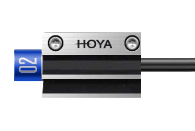
UV-LED spot source AS/AT series |
| Dimension | ø12×50mm (HO-03L~06L lenses included, fixture excluded) |
| Cable length | 2 m (robot cable) |
| Weight | Aprx. 110g (HO-03L~06L lenses included, fixture excluded) |
| Cooling type | nature air cooling |
| Wave length | 365 / 385 / 405 nm |
| Dimming range | 10 ~ 100% |
| Item |
EXECURE-H-1VCIII Controller |
| Dimension | W.90xD.120xH.50mm |
| Weight | approx. 600g |
| Power Supply | DC24V |
| Power Consumption | (AS/AT series) 7.5W/head, Max. 60W with 8 heads |
| Number of Connectable Heads | (AS/AT series) Up to 4 heads *Up to 8 heads with branch cables. |
| Communication | RS-232C |
| Remote Control (Input) | Emergency stop, UV irradiation start/stop |
| Remote Control (Output) | Ready, UV irradiation in progress, Error |
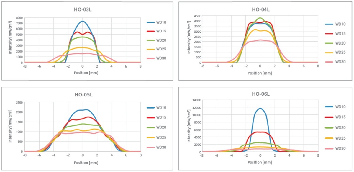
.AS01+main convertible lenses
.AT series (fixed lenses) main model
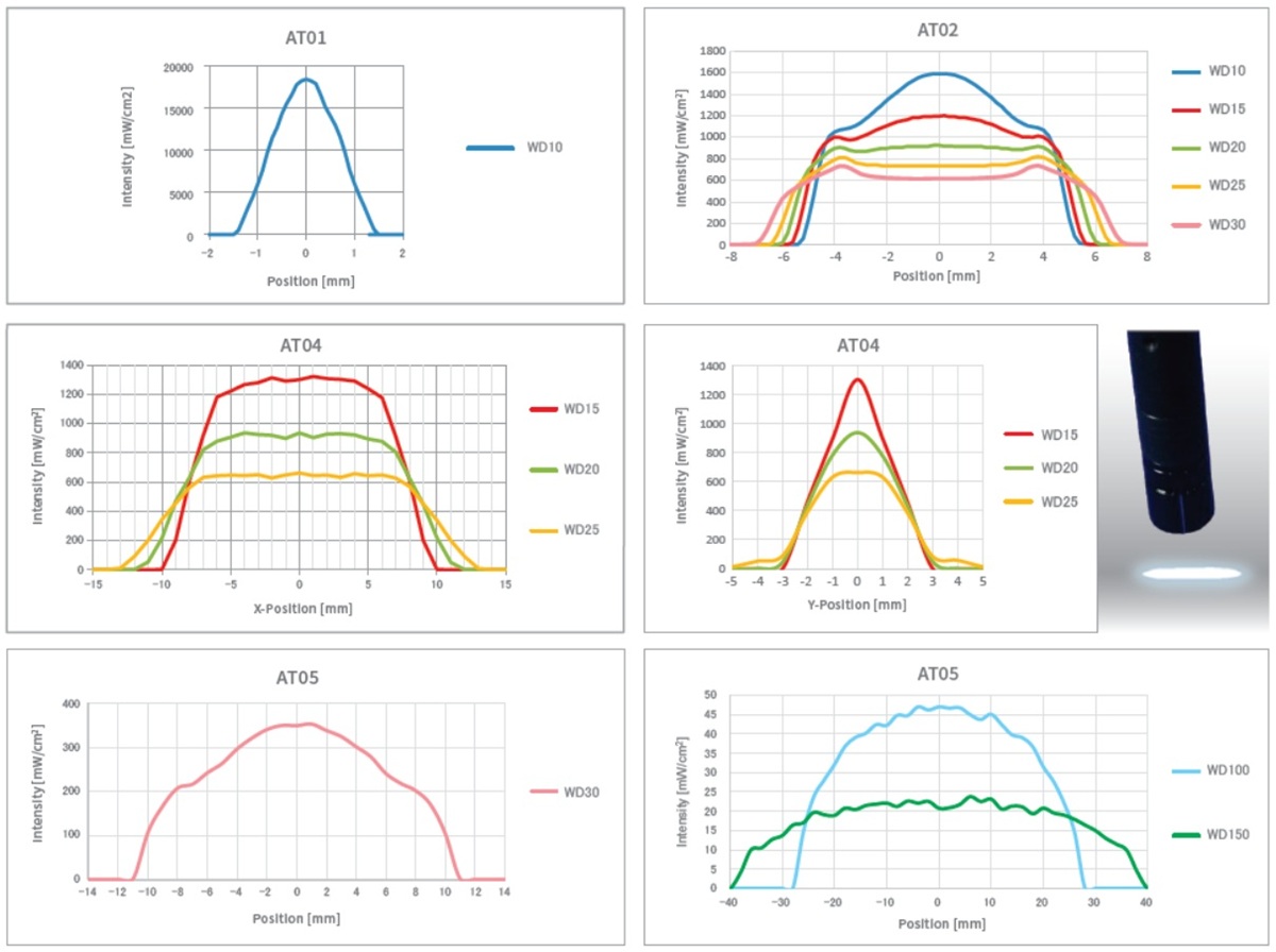
* The above data are all values at 365nm. Please contact us for other wavelengths.
* The above specifications, shapes and strength distribution information are subject to change without prior notice.
* The above specifications, layout and irradiation distribution information are subject to change
* The above distribution graph is a standard value, not a guaranteed value.
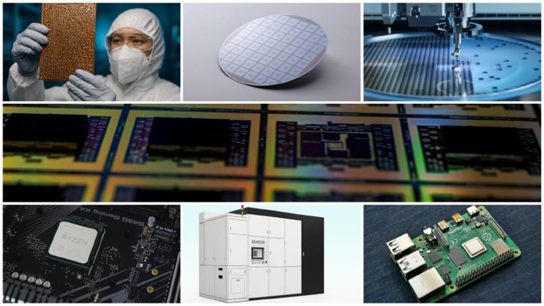
.Examples - semiconductor process lithography, photoresist curing
* Contact us for more information.
 Electronics
 Optoelectronics
 Biotechnology
 Medical Devices
 UV Curing Tech.