
Brief
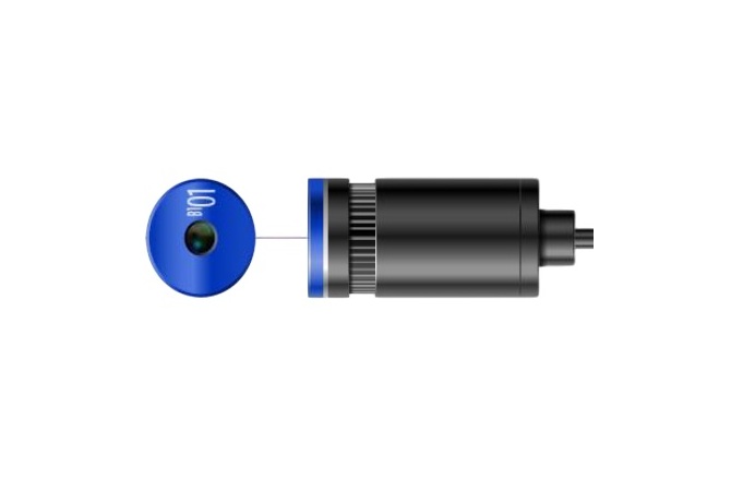
Japan HOYA has won high praise from domestic and foreign customers for its world-leading optical technology, from LEDs to light bulbs, its rich product line and its precise and stable quality. HOYA light source equipment can be widely used in high-precision process fields such as camera module packaging, electronic parts curing, semiconductor exposure process, liquid crystal bonding and medical equipment.
Feature
* By adopting a new chip, its performance is about 1.6 times stronger than the previous model.
* Forced air cooling system (built-in fan) simplifies system construction.
* UV-LED point light source with high UV intensity and large area irradiation.
* The "H-1 VC II" can control up to 2 groups.
.Specification
| Item |
BT-01 | BT-03 | BT-05 |
| Wave length | 365 / 385 / 395 / 405 nm | 365 / 385 / 395 / 405 nm | 365 / 385 / 395 / 405 nm |
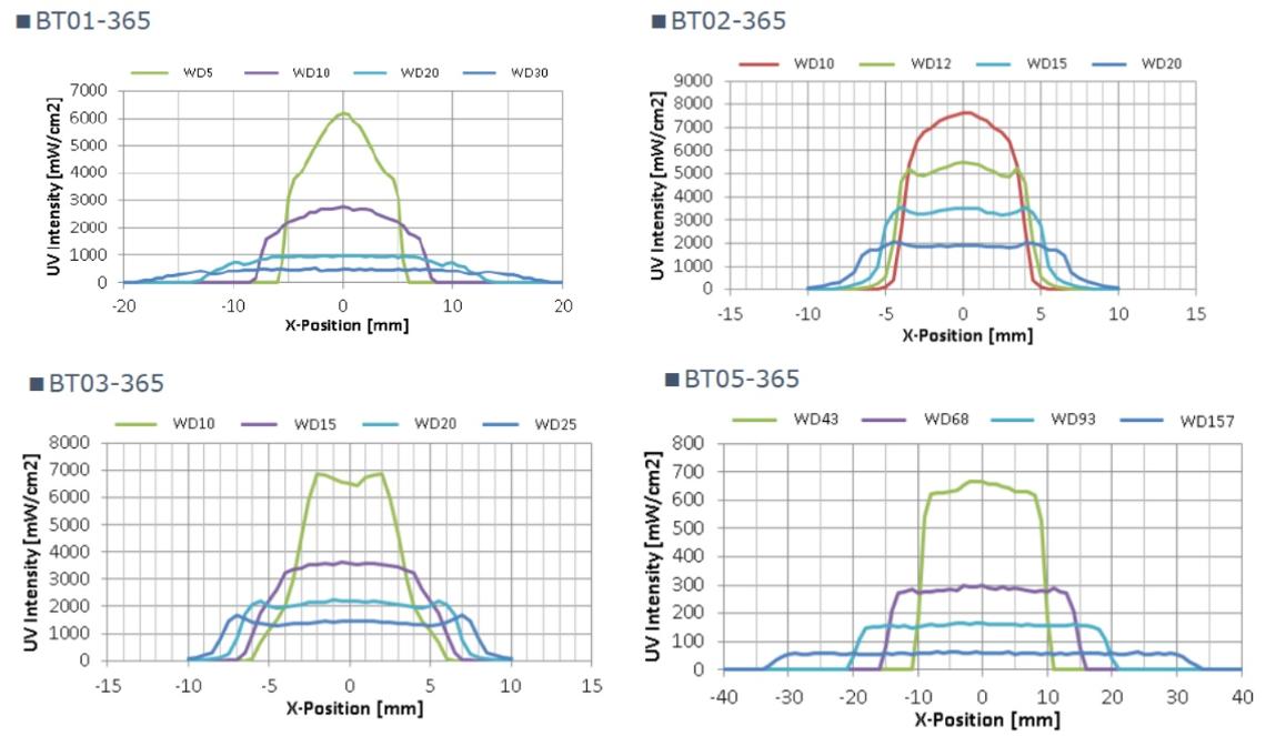
| Initial peak intensity* (mW/cm2) | 2,000(WD10) | 1,500(WD20) | 100(WD93) |
| Cable length | aprx. 2M (robot cable) | aprx. 2M (robot cable) | aprx. 2M (robot cable) |
| Power consumption | 18W | 18W | 18W |
| Weight | 190g | 195g | 305g |
| Material | Lens: Optical glass Radiator and barrel: Aluminum | Lens: Optical glass Radiator and barrel: Aluminum | Lens: Optical glass Radiator and barrel: Aluminum |
| Cooling | forced air cooling | forced air cooling | forced air cooling |
1. Ambient temperature: Operation: +5~+35℃ / 30~85% without condensation or icing;
Storage: -10~-60℃ / 30~85% without condensation or icing
* Initial peak intensity wavelength 365 nm is the value at 365 nm.
* The above specifications, data and information are subject to change and are not guaranteed values.
.BT series Intensity distribution graph
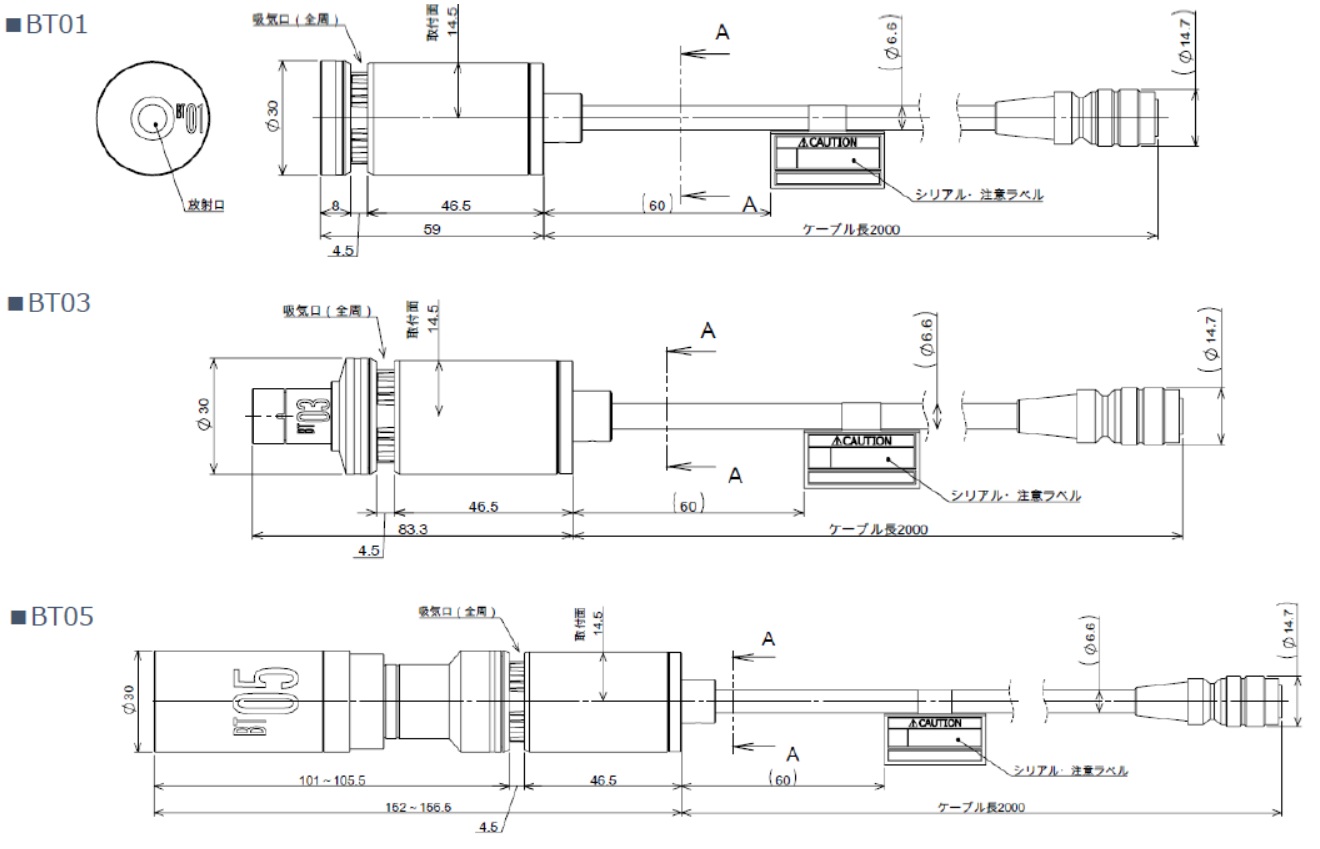
.BT series Layout
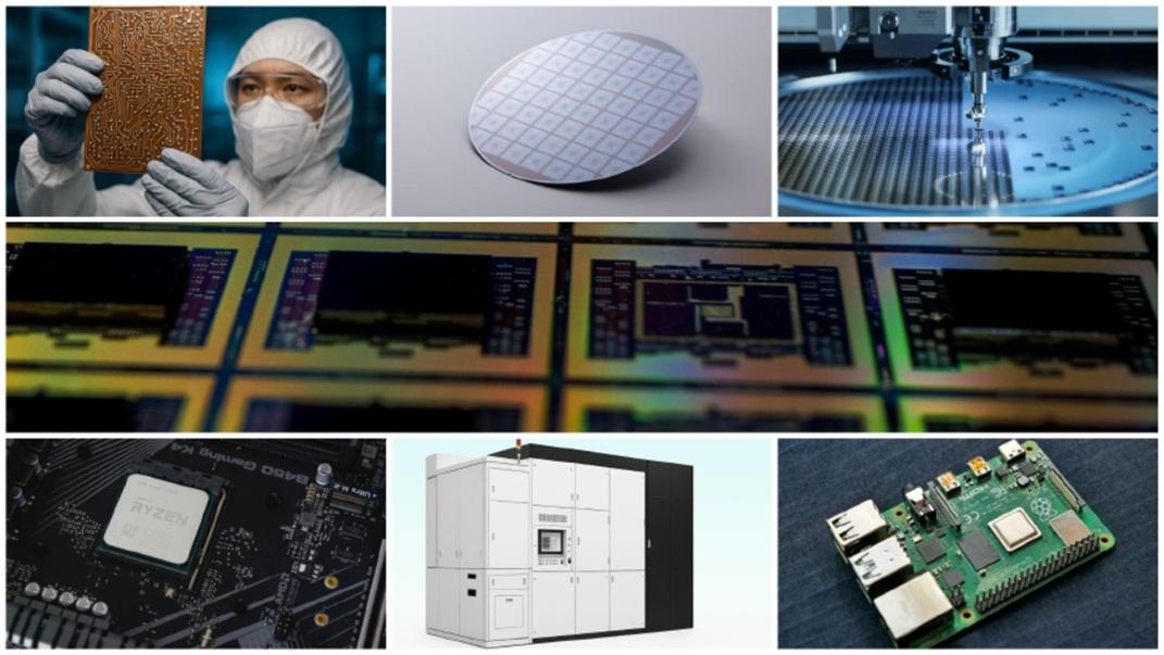
.Examples - Semiconductor process lithography, photoresist curing
* Contact us for more information.
 Electronics
 Biotechnology
 Food and Beverage
 UV Curing Tech.