
Brief
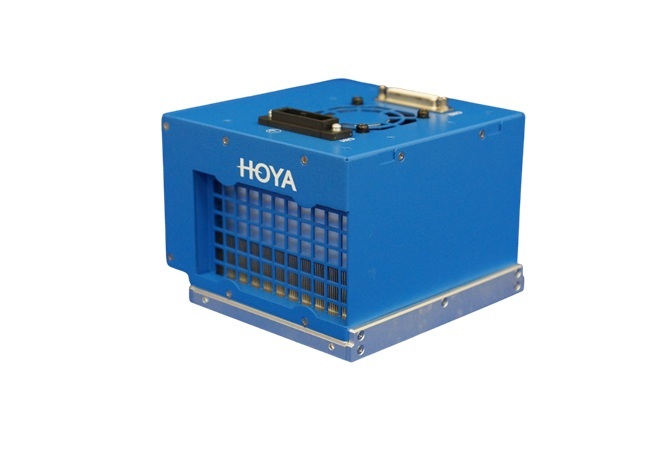
Japan HOYA has won high praise from domestic and foreign customers for its world-leading optical technology, from LEDs to light bulbs, its rich product line and its precise and stable quality. HOYA light source equipment can be widely used in high-precision process fields such as camera module packaging, electronic parts curing, semiconductor exposure process, liquid crystal bonding and medical equipment.
Feature
* Next generation chip system with more than 2 times higher UV intensity than previous models.
* The coverage area is also about 100 square millimeters wider than the original model.
* Connecting two allows for an illumination area of approximately 200 x 100 mm square.
* Built-in drivers allow use without a controller.
.Specification
| Item |
UV-LED area type light source |
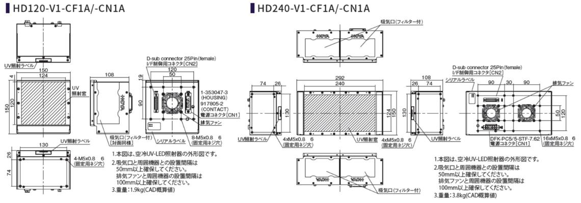
| Dimension (WxDxH) | HD120-V※-CF1A/-CN1A :150×150×108 mm(protrusion part excluded) HD240-V※-CF1A/-CN1A :292×150×108 mm ( protrusion part excluded) |
| Weight | HD120-V※-CF1A/-CN1A :aprx. 1.9 kg(CAD estimated) HD240-V※-CF1A/-CN1A :aprx. 3.8 kg(CAD estimated) |
| Initial peak intensity (WD:5mm) | V1(365nm): 900 / V2(385nm): 1,100 mW/cm2 V4(395nm): 1,100 / V3(405nm): 900 mW/cm2 |
| Cooling type | forced air cooling |
| Wave length | 365(V1)/ 385(V2)/ 395(V4)/ 405(V3) |
| Dimming range | 10 ~ 100% |
| Control type | I/O or RS-485 |
| Input voltage | DC48V |
*The "※" in the model number indicates the wavelength number (1 to 4).
.Intensity distribution graph
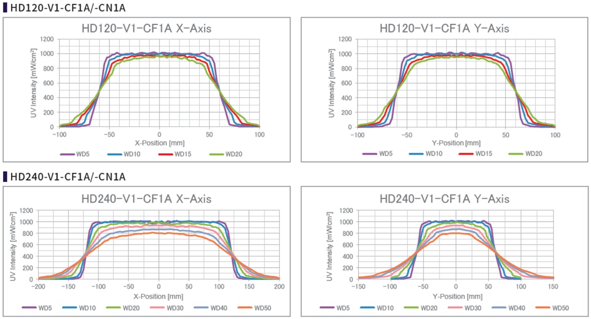 * The above charts are all characteristics of 365nm. Please contact us for other wavelengths.
.HD120 / 240 Layout
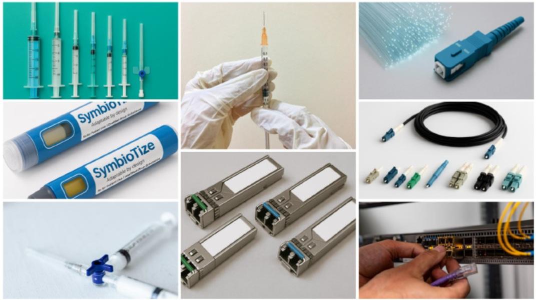
.Examples - Fast curing for medical equipment & packaging, protection of optical communication modules
* Contact us for more information.
 Optoelectronics
 Biotechnology
 Electronics
 Metal Products
 UV Curing Tech.